Voltage-Mode, High-Gain Architecture
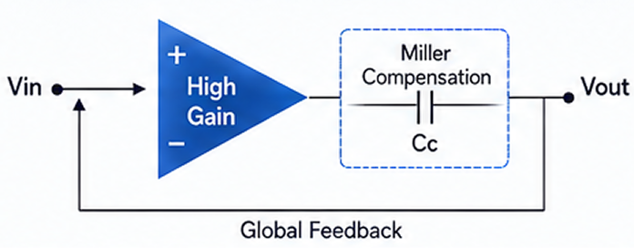
- Requires very high open-loop gain
- Miller compensation limits bandwidth
- Large input RC delay
- Multiple gain stages and more poles
- Higher power consumption and slower response


Current-domain signaling, low-swing transmission, and DC-balanced encoding for short-reach interconnects.
Energy-Efficient · Short-Reach Optimized · Technology-Scalable
H-PHY is designed to minimize CV2 switching energy through ultra-low-swing signaling, enabling energy-efficient, high-bandwidth, and scalable connectivity for wide I/O and next-generation short-reach interconnects.
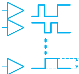
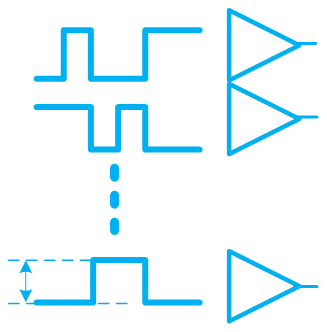
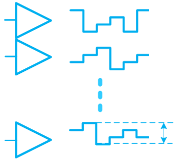
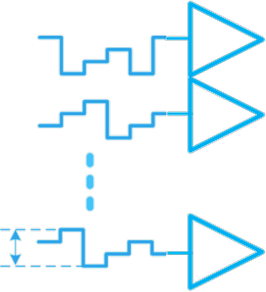
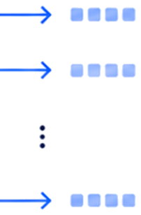
Up to 10x better pJ/bit than conventional PHY
Designed for interposer, package, and chiplet interconnects within short-reach environments
Compact per-channel architecture designed for scalable multi-lane integration
Designed to mitigate SSN, PDN disturbance, crosstalk, jitter, and skew variation
Designed to scale with advanced process nodes and increasing data rates

NRZ Signaling: Reference operating range up to approximately −3 dB channel lossDC-Balanced PAM Signaling: Extended operating range toward approximately −10 dB channel loss in the evaluated configuration
Conceptual illustration. Actual channel-loss tolerance depends on signaling conditions, interconnect characteristics, and system implementation.
S. Han et al., Symp. on VLSI, 2026, pp. 1-3
DOI: 10.1109/VLSITechnologyandCir65830.2026.11577423
View on IEEE Xplore® →
H-PHY employs an RX-centric current-domain architecture based on a Current Conveyor (CC) receiver.
Voltage-Mode, High-Gain Architecture
Current-Mode, Unity Tracking Architecture
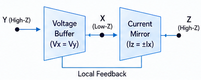
Reduces dependence on conventional gain-bandwidth tradeoffs
No or minimal Miller compensation, supporting wider bandwidth
Reduced sensitivity to interconnect RC effects
Rx ≈ 0 Ω for interconnects
Fewer gain stages,
shorter delay
Faster settling and better stability
Advanced-Node Scalable 10–100 GHz Wideband Operation
Simpler dynamics
and wider bandwidth
Fast settling with reduced propagation delay
Applicable to HBM, chiplet, and Wide I/O interconnects
This Privacy Policy describes how LeadingUI Co., Ltd. (the "Company") collects, uses, and protects personal information in connection with the use of its services.
The Company processes personal information for the purposes below and does not use it for any other purpose. Where the purpose changes, the Company will take necessary measures such as obtaining separate consent.
The Company retains and uses personal information within the period required by applicable law or the period consented to at the time of collection, and destroys it without delay once the purpose has been achieved.
When personal information becomes unnecessary, such as after the retention period has elapsed or the purpose has been achieved, the Company destroys it without delay.
The data subject may at any time exercise the right to request access to, correction of, deletion of, or suspension of the processing of their personal information.
The Company designates a data protection officer who is responsible for overseeing personal information processing and for handling related complaints and remedies from data subjects.
This Privacy Policy applies from its effective date. Any additions, deletions, or corrections arising from changes in law or policy will be announced at least 7 days before they take effect.
Effective date: January 1, 2026
These Terms set out the conditions and procedures for using the services provided by LeadingUI Co., Ltd. (the "Company"), as well as the rights, obligations, and responsibilities of the Company and users, and other necessary matters.
These Terms take effect for all users who wish to use the Service. The Company may amend these Terms where necessary, and amended Terms take effect upon announcement on the notices page.
The Company provides the following services.
The Company may temporarily suspend the Service in the event of maintenance, replacement or failure of information and communication equipment, or interruption of communications.
Users must not engage in the following:
Copyright and other intellectual property rights in works created by the Company belong to the Company. Users must not reproduce, transmit, publish, distribute, broadcast, or otherwise use, for commercial purposes, information obtained through the Service without the Company's prior consent, nor allow any third party to do so.
The Company is exempt from responsibility for providing the Service where it cannot do so due to force majeure or equivalent circumstances. The Company is not liable for any service disruption attributable to the user.
Any lawsuit arising from a dispute between the Company and a user shall be subject to the exclusive jurisdiction of the court having jurisdiction over the location of the Company's head office.
These Terms are effective from January 1, 2026.